Graphene Makes Waves

Scientists at FAU demonstrate the unique relaxation of stress in bilayer graphene
Regardless of whether coming from an internal or external source, high pressure often leads to a state of stress. This not only applies to us humans, but also to materials. Stress in a material is manifested as tensile, compressive or shear forces. On the one hand, these can result from an externally applied load. On the other, stresses can arise from material defects or are due to one part of the material preventing the expansion or contraction of another. What happens to the internal stress of a material which consists of just two atomic layers? This question was considered by FAU researchers.
In the latest issue of the leading scientific journal Nature¹ they report how internal stresses in two layers of carbon, also known as bilayer graphene, relax in a quite startling fashion. The results not only provide deep insight into the interplay of defects and mechanical stresses in nanomaterials but may also open the door to new concepts of tailoring the electronic structure of bilayer graphene and other ultrathin layered crystals.
The interdisciplinary team, which comprises materials scientists, physicists and computer chemists, have explained their unusual observations by comparing the results of detailed electron microscopical analyses with computer simulations.
A Suspended Graphene Membrane for Electron Microscopical Investigation
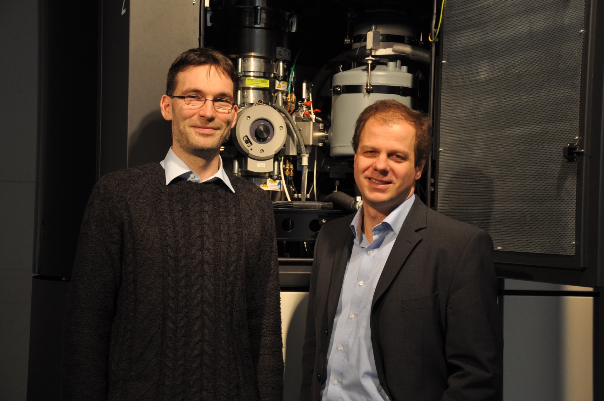
The team first produced high quality bilayer graphene at 1750 °C on atomically flat single crystals of silicon carbide. Using an ingenious approach developed in the group of physicist and co-author Prof. Heiko Weber it was possible to remove the silicon carbide in certain locations without damaging the graphene. “The resulting bilayer membranes are perfect for analysis in the transmission electron microscope because they are fixed in a solid frame of silicon carbide, rather like the jumping mat of a trampoline” explain Dr. Benjamin Butz and Prof. Erdmann Spiecker from the Erlangen-based electron microscopy group which carried out the investigation.
For their microscopic studies the scientists used a state-of-the-art aberration-corrected transmission electron microscope which enabled the fragile graphene bilayers to be studied at reduced electron energy so as to avoid damaging them. During the examination of the samples, the Erlangen researchers made the surprising discovery that instead of perfect bilayer graphene in which atoms are arranged in a periodic lattice with the two layers having a uniform offset from one another, a series of regularly spaced linear defects, also known as “dislocations” were observed.
“Such defects appear when one of the growing atomic layers of bilayer graphene forms in an expanded or contracted fashion in comparison to the other” explains Prof. Spiecker. “If that happens then the two layers do not stack perfectly since one must accommodate more atoms than the other.” However, since bilayer graphene prefers a certain stacking pattern in order to minimize energy, it tries to achieve this over as wide an area as possible. As a result stripes of material appear alternating between perfect stacking with almost no internal stress and out-of-alignment layers with high internal stress. In the latter regions dislocations can be found. The concentration of internal stress at dislocations is a fingerprint of this type of defect, which plays an extremely important role in the investigation and engineering exploitation of crystalline materials.
Relaxation of Stress through Wave Formation
Can a membrane just two atomic layers thick resist the high internal stresses produced at dislocations? The answer is a definite “no” as the Erlangen team could prove. “Since the membrane is so thin, it can readily bend in order to relax the internal stresses”, explains Dr. Butz. To confirm that this indeed occurs, the experimental results were compared with computer simulations which were performed by the group of Prof. Bernd Meyer at the Computer Chemistry Center. In the computer model, the same arrangement of atoms around a dislocation was considered. Here, every single carbon atom, together with its bonds within the atomic layer, was represented in addition to the somewhat weaker interactions between the two layers.
In order to minimize the total energy of the system (a condition which the material tries to attain as long as no external forces are applied) the membrane was found to deform itself in a wave-like manner with one wave formed for each dislocation. “The remarkable thing is that through the formation of waves, the concentration of stress at the dislocations is almost entirely eliminated,” explains Prof. Meyer.
Fundamental Understanding of Dislocations – Effects on Electronic Properties
The results of the Erlangen team have wide-reaching implications for research, not only of graphene but also of related materials such as boron nitride or the dichalcogenides. “Currently attempts are being made to deliberately engineer stress conditions in bilayer graphene in order to tailor the electronic properties of the material.” explains Dr. Butz. “The dislocations and the mechanism by which bilayer graphene deals with internal stress could open the door to entirely new concepts.”
Beyond this, the results from Erlangen are a significant contribution to the understanding of the behaviour of dislocations in nanomaterials, already a hot topic in materials- and nanoscience. “Bilayer graphene is the thinnest material which can host such extended dislocations and is therefore expected to show the most pronounced relaxation of dislocation-related stress”, acknowledges Prof. Spiecker. “It is therefore an ideal model system in which to study the interaction of dislocations with free surfaces.”
Success Story Resulting from an Interdisciplinary Collaboration
The wide-reaching research results only came about due to close cooperation between Erlangen-based scientists from quite different backgrounds: The fabrication of the membranes in the Physics Department, the microscopical analysis and crystallographic interpretation in the Materials Science and Engineering Department and the atomic modelling in the Computer Chemistry Center.
Such interdisciplinary activities have become very much the norm rather than the exception at FAU and continue to receive significant support from the German Science Foundation (DFG) in the framework of its various coordinated progammes, in the present case the Collaborative Research Center “Synthetic carbon allotropes” (SFB 953) and the Cluster of Excellence “Engineering of Advanced Materials” (EXC 315).
¹ Dislocations in Bilayer Graphene, B. Butz, C. Dolle, F. Niekiel, K. Weber, D. Waldmann, H. B. Weber, B. Meyer and E. Spiecker, Nature (2013), DOI: 10.1038/nature12780.
Further Information:
Prof. Erdmann Spiecker
Electron Microscopy Group
Department of Materials Science and Engineering
Cauerstr. 6
91058 Erlangen
Tel. 09131/85-28603
erdmann.spiecker@ww.uni-erlangen.de
www.em.techfak.uni-erlangen.de