An unexpected spin-off of the quantum tunnelling effect: conductivity enhanced by defects
FAU-based researchers solve an enigma of solid state physics
Researchers at FAU and the Max Planck Institute (MPI) in Halle have managed to find the answer to one of the riddles of solid-state physics. The results of their work recently appeared in the prominent journal Nature Communications (DOI: 10.1038/s41467-017-00397-8).
One of the fundamental phenomena of quantum physics is the fact that electrons appear to be able to tunnel through barriers that, to all intents and purposes, should be impenetrable. However this effect, which makes use of the wave-like nature of matter, is operative over very short distances only – for instance less than a nanometre in terms of individual atoms observed under a scanning tunnelling microscope – because of the exponential decay of the wave function within the barrier.
Thus, it was all the more surprising when, some ten years ago, it was discovered that an electrical current would flow for distances up to a thousand times longer in single and double layers of graphene – in other words, a layer of graphite with a thickness of one or two atoms – actually because of this exponential decay of wave functions. This new mechanism of electron transport, however, was difficult to analyse because it was barely distinguishable from the normal transport of electrons in a standard conductor.
Initially, it seemed the effect had been clearly understood, but it soon turned out to be much more complicated when a number of sensational experiments showed that seemingly identical double layer samples proved to be either very conductive or, quite the opposite, had a high level of resistivity. Solid-state physics was facing a puzzle. A number of well-received papers proposed that there must be exotic undiscovered new states of matter, although the theories were based on the resistivity observed only.
Theory of electron transport in defective double layers
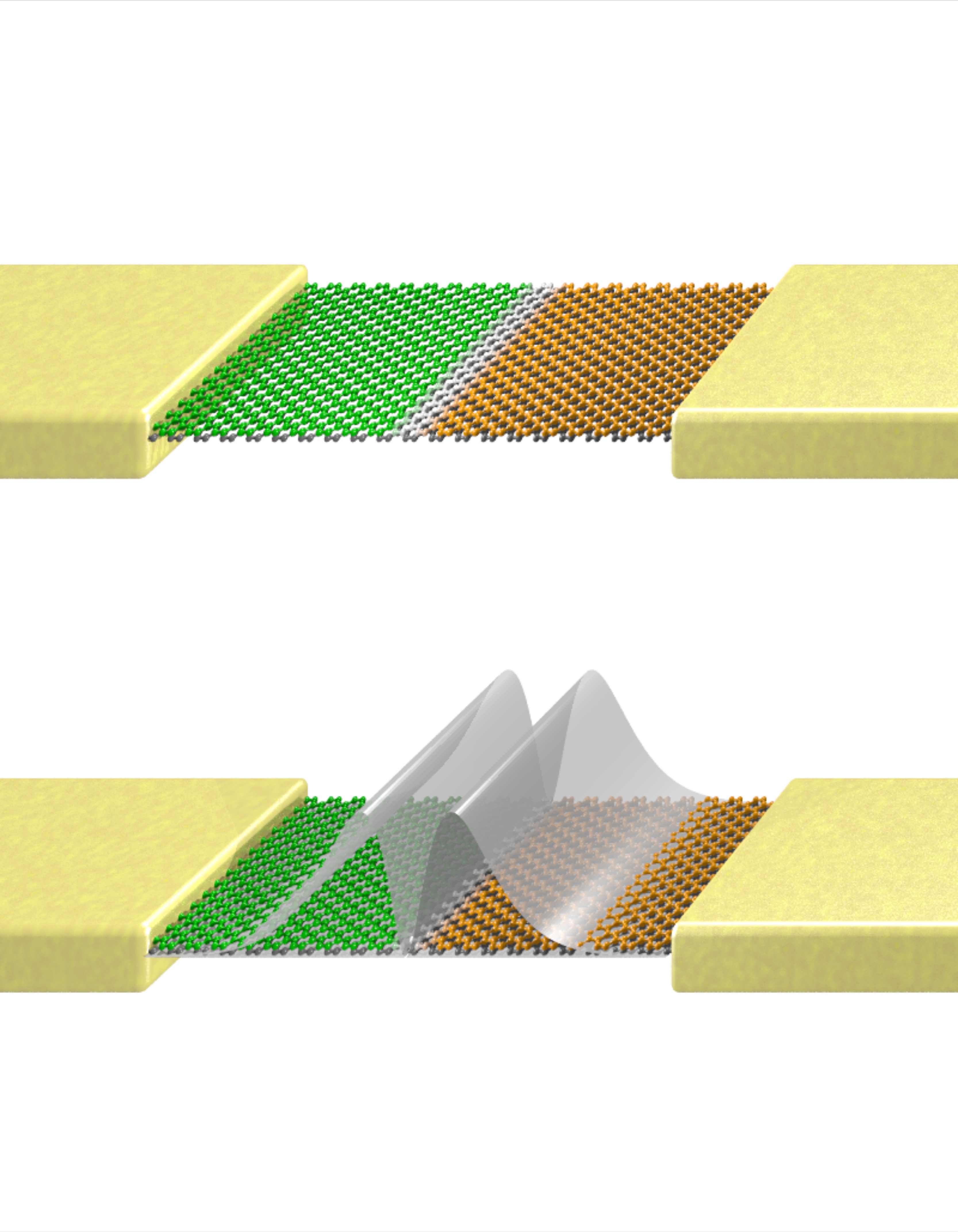
While world-wide research in the field focused on explaining the phenomena on the assumption that the material itself was perfect, FAU-based researchers Dr. Sam Shallcross and Prof. Heiko B. Weber in cooperation with Dr. Sangeeta Sharma of MPI in Halle decided to go down a different route. They developed a theory whereby electron transport was occurring because of defects in these double layers, particularly because of stacking errors that can be compared to the creases in a two-layered table cloth.
Partial dislocations of this nature in graphene double-layers were discovered and analysed a few years ago at FAU. A new method of calculating the electronic structure in double layers, the first that was capable taking precisely these stacking errors into consideration, was developed for the theory. When this method is applied to a double layer of graphene, a new kind of electron transport can be posited that has a mathematical form like that of tunnelling but which is based on a qualitative new concept in physics – the assumption that, under certain circumstances, current can flow more efficiently if there are obstacles in the way.
Shallcross, Sharma and Weber discovered much to their own amazement that, depending on positioning, this electronic structure can behave either as a conductor or an insulator, hence explaining the perplexing results of the previous experiments. They have thus produced a comprehensive explanation of the entire phenomenology of graphene double layers with no need to postulate the existence of exotic new states.
This theoretical concept can be applied to many examples of an entire material class, namely the new and exciting two-dimensional materials. Their findings also serve to point out the fundamental differences in charge transport in our familiar three-dimensional world and the world of two-dimensional materials.
The research was undertaken in the Collaborative Research Centre 953, ‘Synthetic Carbon Allotropes’.project.
Further information:
Prof. Dr. Heiko Weber
Phone: +49 9131 8528421
heiko.weber@fau.de